top of page
접속이온빔 주사전자현미경
(FIB-SEM)
DB550 은 나노분석 및 시료준비를 위한 FIB(Focused Ion Beam) 컬럼을 적용한 FE-SEM(Field Emission-SEM)으로 ‘SuperTunnel’ 전자광학기술과 무자성 대물렌��즈 설계가 적용되어 나노규모의 분석능력을 보장하는 저전압 및 고해상도 이온 컬럼 입니다. 이온 컬럼은 Ga+ 액체 금속 이온원으로 고도로 안정적이고 고품질의 이온 빔으로 용이하게 나노급 제작 능력을 보장합니다.
DB550은 Nano-manipulator, 가스주입시스템, 대물렌즈용 전기 오염방지 메커니즘, 24개의 확장포트를 통합하여 종합적인 구성과 확장성을 갖춘 만능 나노분석 및 제작 플랫폼 입니다.

■ 특징
▶ 저전압, 고해상도
• Super-Tunnel electron optics
• 전자의 광학 경로 교차 제거: 렌즈의 수차를 줄이고 해상도 향상
• 전자기 & 정전기 복합 대물렌즈 사용: 수차 감소 및 저전압 해상도 향상
• Space charge effect 감소: 저전압 해상도 우수
• System 수차 감소
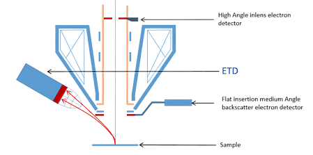
▶Inlens on-axle electron detector

▶Side mounted ETD
▶ Focused ion beam column
• 분해능: 3nm @ 30kV
• Probe current(Ion beam
current range): 1pA ~ 65nA
• 가속 전압 범위: 0.5 ~ 30kV
• 이온 소스 교환 간격: ≥ 1000h
• 안정성: 72 시간 연속 작동


▶ Nanomanipulator
• 챔버 내부 설치
• 3-axis full piezoelectric dirve
• Step 정확도: ≤ 10nm
• 최대 이동 속도: 2mm/s
• 통합제어모드
▶ Gas Injection System (GIS)
• 단일 가스 주입 시스템
• 다양한 가스 공급원
• 접이(Retractable) 거리: ≥ 35mm
• 반복 위치 정확도: ≤ 10um
• 가열 온도 제어 정밀도 ≤ 0.1ºC
• 난방 온도 범위: 실내 온도: ~90ºC
• 통합제어모드

▶ SEM과 동일한 플랫폼에서 소프트웨어 운영
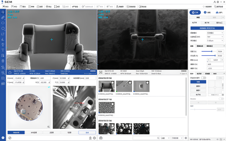
▶ 가스 주입, 조작, 기타 기능 통합 운영 및 실시간 확인

▶ 섹션 구조 관찰
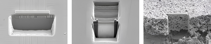
Chip
Chip
Battery
▶ TEM lamella preparation (Sample: Ferritic martensitic steel)
1. Use Pt to deposit
protective layer
2. Simple prepartion of
thin slices using coarse
and fine cutting
3. L cut, nano-manipulator welding is performed
4. After the welding
completed, the sample
connection is cut off


8. TEM observation
7. Final thinning
6. Weld the sample to
the copper column
5. Nanomanipulator
extraction status
▶ TEM lamella (Sample: Ferritic martensitic steel)

DB550 SEM image
TEM atomic image(STEM-HAADF)
■ 규격

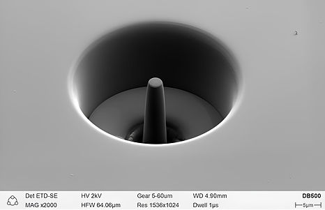
Images gallery
Silicon dioxide spheres (3kV, ETD-SE)

Ion etching
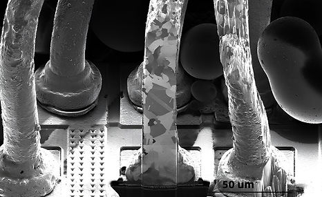
Gold Wire (30kV, ETD)

APT 3D reconstruction
and chemical element analysis

Pt deposition

IC chip #1 (1kV, ETD)
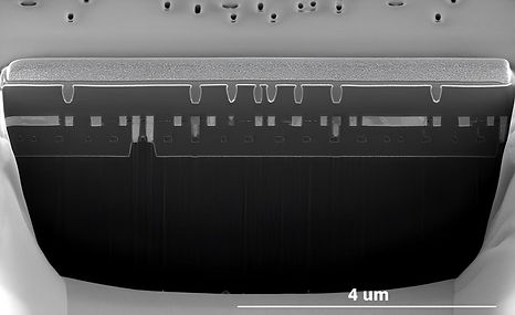
IC chip #2 (1kV, ETD)

bottom of page